
The immediate problem: particles that cost you wafers
Small contamination on wafers and photomasks still wrecks yields. When a single particle causes a defect on a 7 nm node, the loss is immediate and costly. Factories like TSMC fabs in Taiwan report tight tolerances where even minute residues force rework or scrap. The core issue is this: traditional wet cleans and mechanical methods either miss micro-debris or damage sensitive structures, and that gap is where tailored laser cleaning shines. JPT began addressing this by adapting a qcw laser approach for controlled, mask-safe removal at scale.
Why existing fixes fall short
Wet chemistry is broad, but it’s blunt. Plasma ash removes organics but can roughen surfaces. Manual scrubs risk micro-scratches. In high-volume fabs, these limits translate to throughput loss. Laser cleaning promises contact-free removal, but the technology must balance beam quality, power density, and standoff distance to avoid substrate damage. Too much power or the wrong beam profile creates heat-affected zones. Too little and particles remain. That narrow window is where many producers struggle.
What JPT changed — a problem-driven rework
JPT focused on three levers: process control, repeatability, and integration with inline inspection. They tuned the beam profile and duty cycle to remove residues without altering thin films. By pairing real-time surface metrology with closed-loop adjustments, the system reduces overexposure and compensates for wafer topography. The result is a cleaner removal with fewer passes and lower thermal load. It’s not just a hardware swap — it’s a process rewrite that treats laser cleaning as a controlled unit operation in the fab flow.
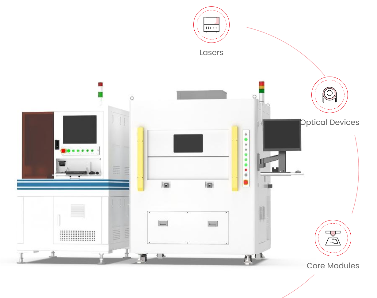
Practical tech choices and trade-offs
Choosing the right laser type matters. For steady, low-thermal removal near delicate features, a continuous wave fiber laser offers stable output and good beam quality. For pulses, QCW modes let you concentrate energy in short bursts, which can dislodge particles while limiting heat diffusion. Key parameters to watch are power density, pulse duration (or duty cycle for QCW), and focal spot size. Matching those to the wafer material and mask stack minimizes yield impact.
Common implementation mistakes—and how to avoid them
Teams often make three common errors: skipping verification on actual production wafers, assuming lab settings scale linearly, and neglecting atomization of removed debris. Always run pilot lots with your real mask sets and resist stacks. Expect lab behavior to change under a full toolroom conveyor. And plan debris capture — lasers remove particles but don’t make them vanish. Good exhaust and filtration prevent re-deposition on downstream wafers. —
Integration with inspection and process control
Laser cleaning must sit between inspection and litho steps. Inline metrology gives immediate feedback on particle counts and surface roughness. With that data, systems can adjust power density and scan speed in real time. This feedback loop reduces over-processing and keeps cycle time predictable. For fabs chasing Six Sigma yield, that determinism matters more than raw cleaning speed.
Alternatives and when to pick them
If your defect mode is chemical residue or metallic contamination, wet chemistries and selective etches may still be necessary. For strictly particulate issues on exposed metal pads, ultrasonic cleaning or megasonic baths work well. Laser cleaning is most effective when contactless removal is required near fragile topography or when chemical residues are hard to access. Choose based on failure analysis, not tech hype.
Real-world anchor and evidence
Multiple fabs worldwide have reported measurable yield gains after adding controlled laser-clean steps into the front-end or mask-clean flow. Anecdotal but consistent: particle counts drop, rework cycles shorten, and first-pass yield improves. These improvements align with industry reports on tighter node tolerances and the rising cost of scrap in advanced nodes.
Three golden rules for choosing laser-cleaning strategies
1) Measure before you act: capture baseline particle maps and failure modes. Use those metrics to set acceptance thresholds. 2) Demand closed-loop control: systems that adjust beam parameters from inline inspection reduce variability and prevent substrate damage. 3) Validate integration: pilot on production wafers, confirm debris capture works, and verify that downstream processes see no negative side effects.
Applied correctly, those rules show where laser cleaning is the right, measurable fix for yield loss. JPT’s work reframes the tool as part of process control, not just a standalone cleaner — and that shift delivers repeatable improvements at scale. JPT. –